


Semiconductor CNC Machining
Parts for Chip Equipment are Finer Than a Hair
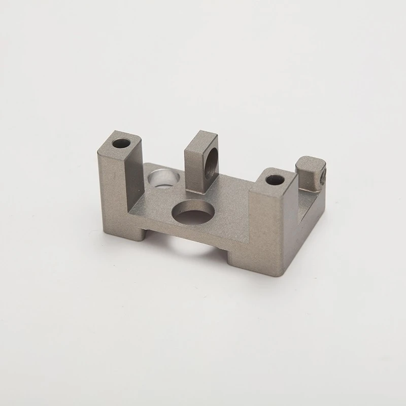
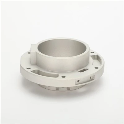
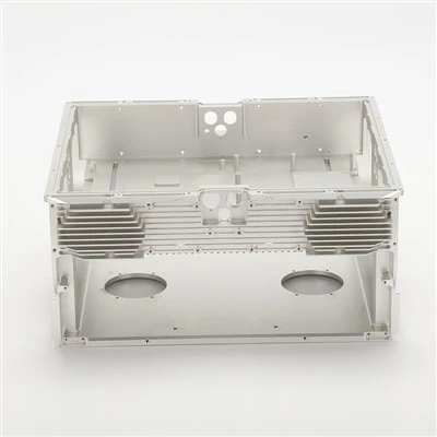
Wafer transfer arms, vacuum chambers, and probe station parts require extreme cleanliness, precision, and material purity. Hayi Technology's semiconductor cnc machining service machines stainless steel, aluminum, engineering ceramic, and PEEK in a clean environment. Dimension tolerance is ±0.005mm. Surface roughness is Ra ≤0.4μm. For example, a semiconductor equipment maker needed a PEEK wafer guide ring. The surface could not have burrs larger than 0.01mm. We used high speed milling and manual deburring. The part passed the client's microscope inspection. This case shows semiconductor parts need both precision and cleanliness. Our MOQ is 1 piece.
|
Parameter |
Details |
|
Minimum Order Qty |
1 piece |
|
Sample Time |
1 day minimum |
|
Batch Lead Time |
~15 days |
|
Dimension Tolerance |
±0.005mm |
|
Surface Roughness |
Ra ≤0.4μm |
|
Cutting Method |
Minimum quantity lubrication or dry cutting (no oil contamination) |
|
Materials |
Aluminum 6061/7075, stainless 304/316L/17-4PH, PEEK, PPS, ceramic |
|
Post-Processing |
Ultrasonic cleaning, vacuum packaging |
|
Inspection |
CMM measurement, photo documentation per part |
|
Certification |
ISO9001:2015 (Cert No. 19925Q02204R0S) |
Oil-Free Machining and Ultrasonic Cleaning
We use minimum quantity lubrication or dry cutting to avoid oil contamination on the parts. Common materials are aluminum (6061, 7075), stainless steel (304, 316L, 17-4PH), PEEK, PPS, and ceramic. After machining, parts go through ultrasonic cleaning and then vacuum packaging. We hold ISO9001:2015 certification. Each part is CMM measured and photo documented. Before packing, we do 100% full inspection. We also accept third-party inspection. Our semiconductor cnc machining service is fast for prototyping.

Fast Samples, 1 Day Minimum
The semiconductor industry has fast product iteration and needs quick samples. Our custom sample time is 1 day minimum. Batch lead time is about 15 days. Payment: 50% deposit for custom development. Trade terms: EXW, FOB, DDP. During production, we send photo or video updates. If any problem occurs, we talk immediately and improve after we find the cause. We have a dedicated after-sales person. Semiconductor equipment makers have strict requirements for suppliers, but once approved, the relationship is stable. Our technicians can help you select contamination-free processes. You can get a ticket to enter the semiconductor supply chain with our help.
Hot Tags: semiconductor CNC machining, China semiconductor CNC machining manufacturers
You Might Also Like


Send Inquiry