


Precision Machining for Semiconductor Equipment
Vacuum Chambers and Electrodes Must Be Absolutely Airtight
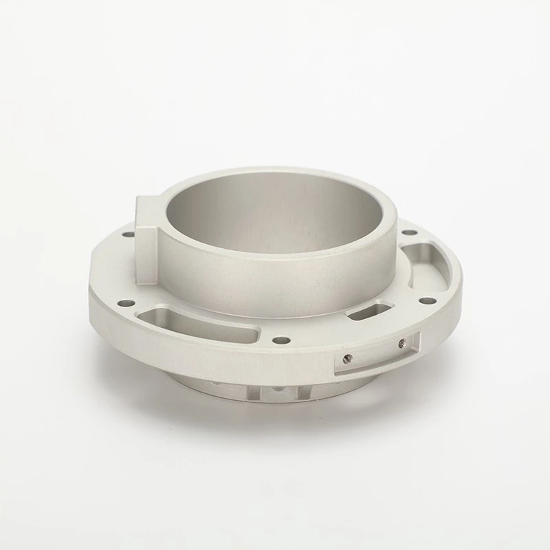
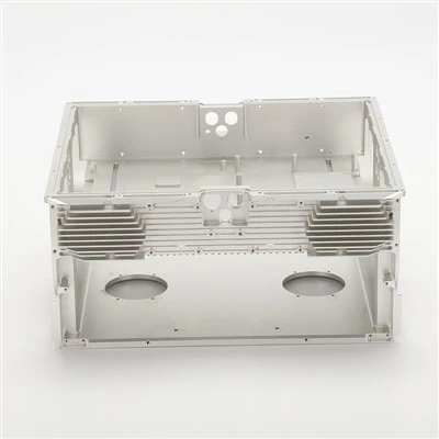
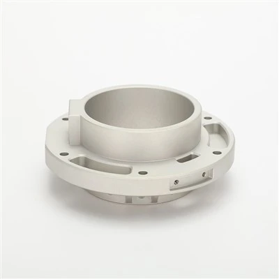
Semiconductor etching and deposition equipment use vacuum chambers, heater plates, and electrodes. They require pure materials, no pores, and high flatness. Hayi Technology's precision machining for semiconductor equipment machines aluminum and stainless steel vacuum parts. Flatness can reach 0.01mm per meter. Surface roughness can reach Ra ≤0.8μm. For example, a semiconductor equipment company needed an aluminum heater plate with diameter of 400mm and flatness of 0.01mm. We used double-sided grinding and met the requirement. The client said temperature distribution uniformity improved significantly. This case shows flatness of vacuum parts decides process uniformity. Our MOQ is 1 piece.
|
Parameter |
Details |
|
Minimum Order Qty |
1 piece |
|
Sample Time |
1 day minimum for small parts |
|
Batch Lead Time |
15-20 days for large parts |
|
Materials |
6061-T6 aluminum (anodized), 304/316L stainless steel (electro-polished) |
|
Equipment |
Large gantry mill (1.5m travel), precision grinder |
|
Flatness Capability |
0.01mm per meter |
|
Surface Roughness |
Ra ≤0.8μm |
|
Helium Leak Test |
Leak rate ≤1×10⁻⁹ Pa·m³/s |
|
Inspection |
Flatness report, leak test report per part |
|
Certification |
ISO9001:2015 (Cert No. 19925Q02204R0S) |
Aluminum and Stainless Steel Vacuum Parts, Helium Leak Tested
We use 6061-T6 aluminum (surface anodized) and 304/316L stainless steel (electro-polished). Our large gantry mill has travel of 1.5 meters. We also have precision grinders. All vacuum parts get a helium mass spectrometer leak test. Leak rate is ≤1×10⁻⁹ Pa·m³/s. We hold ISO9001:2015 certification. Each part comes with a flatness inspection report and a leak test report. Before packing, we do 100% full inspection. We also accept third-party inspection. Our precision machining for semiconductor equipment service handles large parts as well.

Large Sizes Also Available, 15 Days Delivery
Semiconductor equipment parts are often large. Our custom sample time is 1 day minimum for small parts. Large parts take 15-20 days. Payment: 50% deposit. Trade terms: EXW, FOB, DDP. During production, we send photo or video updates. If any problem occurs, we talk immediately and improve after we find the cause. We have a dedicated after-sales person. Etching, deposition, and inspection equipment makers have high requirements for machining suppliers. Our technicians can help you design vacuum sealing structures. You can help your clients ensure the reliability of their vacuum systems.
Hot Tags: precision machining for semiconductor equipment, China precision machining for semiconductor equipment manufacturers
You Might Also Like


Send Inquiry